sexta-feira, 26 de janeiro de 2024

TeamGroup Reveals 14GB/s Innogrit IG5666-Based T-Force Ge Pro PCIe 5.0 SSD

Virtually all client SSDs with a PCIe 5.0 x4 interface released to date use Phison's PS5026-E26 controller. Apparently, TeamGroup decided to try something different and introduced a drive powered by a completely different platform, the Innogrit IG5666. The T-Force Ge Pro SSD not only uses an all-new platform, but it also boasts with fast 3D NAND to enable a sequential read speed of up to 14 GB/s, which almost saturates the PCIe 5.0 x4 bus.

TeamGroup's T-Force Ge Pro PCIe 5.0 SSDs will be among the first drives to use the Innogrit IG5666 controller, which packs multiple cores that can handle an LDPC ECC algorithm with a 4096-bit code length, features low power consumption, has eight NAND channels, is made on a 12 nm-class process technology, and has a PCIe 5.0 x4 host interface. The drives will be available in 1 TB, 2 TB, and 4 TB configurations as well as will rely on high-performance 3D TLC NAND memory with a 2400 MT/s interface speed to guarantee maximum performance.

Indeed, 2 TB and 4TB T-Force Ge Pro drives are rated for an up to 14,000 MB/s sequential read speed as well as an up to 11,800 MB/s sequential write speed, which is in line with the highest-end SSDs based on the Phison E26 controller. Meanwhile, TeamGroup does not disclose random performance offered by these SSDs.

What is noteworthy is that to T-Force Ge Pro drives are equipped with a simplistic graphene heatspreader, which is said to be enough to sustain such high-performance levels under loads. Usage of such a cooler makes it easy to fit a T-Force Ge Pro into almost any system, a major difference with many of Phison E26-based drives. Of course, only reviews will reveal whether such a cooling system is indeed enough to properly cool the SSDs, but the fact that TeamGroup decided to go with a thin cooler is notable.

TeamGroup is set to offer its T-Force Ge Pro SSDs with a five-year warranty. Amazon, Newegg, and Amazon Japan will start taking pre-orders on these drives on February 9, 2024. Prices are currently unknown.


from AnandTech https://ift.tt/lCdf8jB
via IFTTT

quinta-feira, 25 de janeiro de 2024

Intel Teams Up with UMC for 12nm Fab Node at IFS

Intel and UMC on Thursday said they had entered into an agreement to jointly to develop a 12 nm photolithography process for high-growth markets such as mobile, communication infrastructure, and networking. Under the terms of the deal, the two companies will co-design a 12 nm-class foundry node that Intel Foundry Services (IFS) will use at its fabs in Arizona to produce a variety of chips.

The new 12 nm manufacturing process will be developed in Arizona and used in Fabs 12, 22, and 32 at Intel's Ocotillo Technology Fabrication site in Arizona. The two companies will jointly work on the fabrication technology itself, process design kit (PDK), electronic design automation (EDA) tools, and intellectual properties (IP) solutions from ecosystem partners to enable quick deployment of the node by customers once the tech is production ready in 2027.

Intel's Fabs 12, 22, and 32 in Arizona are currently capable of making chips on Intel's 7nm-class, 10 nm, 14 nm, and 22 nm manufacturing processes. So as Intel rolls out its Intel 4, Intel 3, and Intel 20A/18A production at other sites and winds down production of Intel 7-based products, these Arizona fabs will be freed to produce chips on a variety of legacy and low-cost nodes, including the 12 nm fabrication process co-developed by UMC and Intel.

While Intel itself has a variety of highly-customized process technologies for internal use to produce its own CPUs and similar products, its IFS division essentially has only three: Intel 16 for cost-conscientious customers designing inexpensive low-power products (including those with RF support), Intel 3 for those who develop high-performance solutions yet want to stick to familiar FinFET transistors, and Intel 18A aimed at developers seeking for no-compromise performance and transistor density enabled by gate-all-around RibbonFET transistors and PowerVia backside power delivery. To be a major foundry player, three process technologies are not enough; IFS needs to address as many customers as possible, and this is where collaboration with UMC comes into play.

UMC already has hundreds of customers who develop a variety of products for automotive, consumer electronics, Internet-of-Things, smartphone, storage, and similar verticals. Those customers are quite used to working with UMC, but the best technology that the foundry has is its 14 nm-class 14FFC node. By co-designing a 12 nm-class process technology with Intel, UMC will be able to address customers who need something more advanced than its own 14 nm node, but without having to develop an all-new manufacturing process itself and procuring advanced fabs tools. Meanwhile, Intel gains customers for its fully depreciated (and presumably underutilized) fabs.

The collaboration on a 12 nm node extends the process technology offerings for both companies. What remains to be seen is whether Intel's own 16 nm-class process technology will compete and/or overlap with the jointly developed 12 nm node. To avoid this, we would expect UMC to add some of its know-how to the new tech and make it easier for customers to migrate to this process from its 28 nm-class and 14FFC offerings, which guarantees that the 12 nm node will be used for years to come.

Intel's partnership with UMC comes on the heels of the company's plan to build 65nm chips for Tower Semiconductor at its Fab 11X. Essentially, both collaborations allow Intel's IFS to use its fully depreciated fabs, gain relationship with fabless chip designers, and earn money. Meanwhile, its partners expand their capacity and reach without making heavy capital investments.

"Our collaboration with Intel on a U.S.-manufactured 12 nm process with FinFET capabilities is a step forward in advancing our strategy of pursuing cost-efficient capacity expansion and technology node advancement in continuing our commitment to customers," said Jason Wang, UMC co-president. "This effort will enable our customers to smoothly migrate to this critical new node, and also benefit from the resiliency of an added Western footprint. We are excited for this strategic collaboration with Intel, which broadens our addressable market and significantly accelerates our development roadmap leveraging the complementary strengths of both companies."


from AnandTech https://ift.tt/FegqpVf
via IFTTT

Intel's First High-Volume Foveros Packaging Facility, Fab 9, Starts Operations

Intel this week has started production at Fab 9, the company's latest and most advanced chip packaging plant. Joining Intel's growing collection of facilities in New Mexico, Fab 9 is tasked with packaging chips using Intel's Foveros technology, which is currently used to build the company's latest client Core Ultra (Meteor Lake) processors and Data Center Max GPU (Ponte Vecchio) for artificial intelligence (AI) and high-performance computing (HPC) applications.

The fab near Rio Rancho, New Mexico, cost Intel $3.5 billion to build and equip. The high price tag of the fab – believed to be the single most expensive advanced packaging facility ever built – underscores just how serious Intel is regarding its advanced packaging technologies and production capacity. Intel's product roadmaps call for making significant use of multi-die/chiplet designs going forward, and coupled with Intel Foundry Services customers' needs, the company is preparing for a significant jump in production volumes for Foveros, EMIB, and other advanced packaging techniques.

Intel's Foveros is a die-to-die stacking technology that uses a base die produced using the company's low-power 22FFL fabrication process and chiplet dies stacked on top of it. The base die can act like an interconnection between the dies it hosts, or can integrate certain I/O or logic. The current generation Foveros supports bumps that are as small as 36 microns and can enable up to 770 connections per square millimeter, but as the bumps become 25 and 18 microns eventually, the technology will increase connection density and performance (both in terms of bandwidth and in terms of supported power delivery).

A Foveros base die can be as big as 600 mm2, but for applications that require base dies larger than 600 mm2 (such as those used for datacenter products), Intel can stitch multiple base dies together using co-EMIB packaging technology.

Finally coming into full production, the new Fab 9 (which has inherited its name from what was once a 6-inch wafer lithography fab) is slated to be Intel's crown jewel for Foveros chip packaging for at least the next couple of years. While the company has "advanced packaging" capabilities in Malaysia (PGAT) as well, those facilities are currently only tooled for EMIB production, meaning that all of Intel's Foveros packaging is taking place on its New Mexico campus. As Intel's first high-volume Foveros packaging facility, the additional capacity should greatly expand Intel's total Foveros packaging throughput, though the company isn't providing specific volume figures.

With Intel's Fab 11x directly next door, the pair of facilities are also Intel's first co-located packaging advanced packaging site, allowing Intel to cut down on how many dies they have to import from other Intel fabs. Though as Fab 11x is not an Intel 4 facility, in the case of Meteor Lake it is only suitable for producing the 22FFL base die. Intel is still importing the Intel 4-built CPU die (Oregon & Ireland), as well as the TSMC-manufactured graphics, SoC, and I/O dies (Taiwan).

"Today, we celebrate the opening of Intel's first high-volume semiconductor operations and the only U.S. factory producing the world's most advanced packaging solutions at scale," said Keyvan Esfarjani, Intel executive vice president and chief global operations officer. "This cutting-edge technology sets Intel apart and gives our customers real advantages in performance, form factor and flexibility in design applications, all within a resilient supply chain. Congratulations to the New Mexico team, the entire Intel family, our suppliers, and contractor partners who collaborate and relentlessly push the boundaries of packaging innovation."


from AnandTech https://ift.tt/zpJm26w
via IFTTT

quarta-feira, 24 de janeiro de 2024

Melhores dicas para manter a segurança da sua casa inteligente

Imagem de R ARCHITECTURE por unsplash

As casas inteligentes são muito comuns nos dias que correm devido às inúmeras vantagens, como facilitar a vida dos seus moradores, ajudar a poupar uns euros ou até mesmo o conforto que trazem à habitação. Apesar de minimamente seguras, o uso de dispositivos tecnológicos, só por si, já traz alguns riscos.
A melhor forma de proteger a sua habitação é entender esses riscos e tomar medidas que ajudem a manter, ao máximo, a segurança da habitação. Neste conteúdo vamos partilhar algumas sugestões que farão toda a diferença na segurança da sua casa inteligente.

Como manter a segurança da sua casa inteligente?

1. Use apenas dispositivos necessários

Quanto mais dispositivos inteligentes usar, mais portas de entrada terá para possíveis ameaças de segurança. Antes de comprar qualquer dispositivo, questione-se se realmente precisa dessa nova tecnologia na habitação e lembre-se dos riscos que a mesma pode trazer se a segurança for comprometida.
Por exemplo, a Alexa é um excelente apoio, mas se a segurança for comprometida, lembre-se que essa assistente de voz ouve tudo o que acontece em casa, nunca dorme.

2. Invista um pouco mais na segurança da internet

O Centro Nacional de Cibersegurança de Portugal preocupa-se com as questões de segurança na internet e dá diversos conselhos para que a internet da nossa casa se torne mais segura. Entre eles, destacam-se o alterar o nome da rede (não usar o nome que vem com o router), optar por configurações criptográficas mais seguras ou até mesmo criar uma rede diferente para os convidados.
Ainda falando nestas questões, é possível criar uma rede diferente para os eletrodomésticos inteligentes e usar a rede principal para dispositivos pessoais, como o telemóvel, tablet ou computador. Esta é uma forma de manter, ao máximo, a segurança dos seus dados pessoais e privacidade.

Imagem de BENCE BOROS por unsplash

3. Mantenha o equipamento atualizado

Os equipamentos de há 5 anos são menos seguros do que os equipamentos que usamos nos dias de hoje. Com o avanço rápido que a tecnologia tem sofrido, torna-se apenas natural que cada atualização, seja de software ou hardware, seja mais segura do que a versão anterior.
Sendo assim, se tiver equipamentos antigos, seja de eletrodomésticos, gadgets ou mesmo o router da internet, troque-os por opções mais recentes. Para tornar esta troca mais económica pode vender os produtos anteriores ou levá-los a lojas de produtos em segunda mão.

4. Mantenha a segurança das suas contas

Os dispositivos inteligentes estão associados a contas e, portanto, manter a segurança dessas contas é essencial para a segurança da habitação.
Já falamos neste conteúdo com dicas de segurança para este ano de 2024 sobre algumas recomendações, nomeadamente o uso da autenticação de dois fatores, escolher passwords fortes e até o uso de softwares de segurança nos dispositivos móveis.
Além das dicas desse conteúdo, recomendamos que use uma password única para cada um dos dispositivos inteligentes, evitando, ao máximo, o uso da mesma password em dois dispositivos diferentes. Outra recomendação é alterar a password a cada 60 ou 90 dias, no mínimo.
E, claro, evite aceder às contas em outras redes de internet públicas ou que não sejam seguras ou até mesmo dar acesso a terceiros – o melhor é entrar nas contas, apenas, com a sua rede doméstica e através do seu dispositivo.

5. Esteja atento a quem está a usar a sua rede Wi-Fi

E, por último, recomendamos que esteja atento a quem usa a sua rede Wi-Fi. Existem formas de saber que dispositivos estão ligados à sua internet e até expulsar dispositivos desconhecidos manualmente, o que oferece uma camada de proteção extra se estiver atento.
O nosso conselho é investir num software que não só lhe dê essa informação, como também lhe dê segurança extra. E, claro, torne esta inspeção um hábito, no mínimo, mensal.

Com estas dicas, a sua habitação ficará muito mais segura.

The post Melhores dicas para manter a segurança da sua casa inteligente appeared first on Telemoveis.com.

MLCommons To Develop PC Client Version of MLPerf AI Benchmark Suite

MLCommons, the consortium behind the MLPerf family of machine learning benchmarks, is announcing this morning that the organization will be developing a new desktop AI benchmarking suite under the MLPerf banner. Helmed by the body’s newly-formed MLPerf Client working group, the task force will be developing a client AI benchmark suit aimed at traditional desktop PCs, workstations, and laptops. According to the consortium, the first iteration of the MLPerf Client benchmark suite will be based on Meta’s Llama 2 LLM, with an initial focus on assembling a benchmark suite for Windows.

The de facto industry standard benchmark for AI inference and training on servers and HPC systems, MLCommons has slowly been extending the MLPerf family of benchmarks to additional devices over the past several years. This has included assembling benchmarks for mobile devices, and even low-power edge devices. Now, the consortium is setting about covering the “missing middle” of their family of benchmarks with an MLPerf suite designed for PCs and workstations. And while this is far from the group’s first benchmark, it is in some respects their most ambitious effort to date.

The aim of the new MLPerf Client working group will be to develop a benchmark suitable for client PCs – which is to say, a benchmark that is not only sized appropriately for the devices, but is a real-world client AI workload in order to provide useful and meaningful results. Given the cooperative, consensus-based nature of the consortium’s development structure, today’s announcement comes fairly early in the process, as the group is just now getting started on developing the MLPerf Client benchmark. As a result, there are still a number of technical details about the final benchmark suite that need to be hammered out over the coming months, but to kick things off the group has already narrowed down some of the technical aspects of their upcoming benchmark suite.

Perhaps most critically, the working group has already settled on basing the initial version of the MLPerf Client benchmark around the Llama 2 large language model, which is already used in other versions of the MLPerf suite. Specifically, the group is eyeing 7 billion parameter version of that model (Llama-2-7B), as that’s believed to be the most appropriate size and complexity for client PCs (at INT8 precision, the 7B model would require roughly 7GB of RAM). Past that however, the group still needs to determine the specifics of the benchmark, most importantly the tasks which the LLM will be benchmarked executing on.

With the aim of getting it on PCs of all shapes and sizes, from laptops to workstations, the MLPerf Client working group is going straight for mass market adoption by targeting Windows first – a far cry from the *nix-focused benchmarks they’re best known for. To be sure, the group does plan to bring MLPerf Client to additional platforms over time, but their first target is to hit the bulk of the PC market where Windows reigns supreme.

In fact, the focus on client computing is arguably the most ambitious part of the project for a group that already has ample experience with machine learning workloads. Thus far, the other versions of MLPerf have been aimed at device manufacturers, data scientists, and the like – which is to say they’ve been barebones benchmarks. Even the mobile very of the MLPerf benchmark isn’t very accessible to end-users, as it’s distributed as a source-code release intended to be compiled on the target system. The MLPerf Client benchmark for PCs, on the other hand, will be a true client benchmark, distributed as a compiled application with a user-friendly front-end. Which means the MLPerf Client working group is tasked with not only figuring out what the most representative ML workloads will be for a client, but then how to tie that together into a useful graphical benchmark.

Meanwhile, although many of the finer technical points of the MLPerf Client benchmark suite remain to be sorted out, talking to MLCommons representatives, it sounds like the group has a clear direction in mind on the APIs and runtimes that they want the benchmark to run on: all of them. With Windows offering its own machine learning APIs (WinML and DirectML), and then most hardware vendors offering their own optimized platforms on top of that (CUDA, OpenVino, etc), there are numerous possible execution backends for MLPerf Client to target. And, keeping in line with the laissez faire nature of the other MLPerf benchmarks, the expectation is that MLPerf Client will support a full gamut of common and vendor-proprietary backends.

In practice, then, this would be very similar to how other desktop client AI benchmarks work today, such as UL’s Procyon AI benchmark suite, which allows for plugging in to multiple execution backends. The use of different backends does take away a bit from true apples-to-apples testing (though it would always be possible to force fallback to a common API like DirectML), but it gives the hardware vendors room to optimize the execution of the model to their hardware. MLPerf takes the same approach to their other benchmarks right now, essentially giving hardware vendors free reign to come up with new optimizations – including reduced precision and quantization – so long as they don’t lose inference accuracy and fail meet the benchmark’s overall accuracy requirements.

Even the type of hardware used to execute the benchmark is open to change: while the benchmark is clearly aimed at leveraging the new field of NPUs, vendors are also free to run it on GPUs and CPUs as they see fit. So MLPerf Client will not exclusively be an NPU or GPU benchmark.

Otherwise, keeping everyone on equal footing, the working group itself is a who’s who of hardware and software vendors. The list includes not only Intel, AMD, and NVIDIA, but Arm, Qualcomm, Microsoft, Dell, and others. So there is buy-in from all of the major industry players (at least in the Windows space), which has been critical for driving the acceptance of MLPerf for servers, and will similarly be needed to drive acceptance of MLPerf client.

The MLPerf Client benchmark itself is still quite some time from release, but once it’s out, it will be joining the current front-runners of UL’s Procyon AI benchmark and Primate Labs’ Geekbench ML, both of which already offer Windows client AI benchmarks. And while benchmark development is not necessarily a competitive field, MLCommons is hoping that their open, collaborative approach will be something that sets them apart from existing benchmarks. The nature of the consortium means that every member gets a say (and a vote) on matters, which isn’t the case for proprietary benchmarks. But it also means the group needs a complete consensus in order to move forward.

Ultimately, the initial version of the MLPerf Client benchmark is being devised as more of a beginning than an end product in and of itself. Besides expanding the benchmark to additional platforms beyond Windows, the working group will also eventually be looking at additional workloads to add to the suite – and, presumably, adding more models beyond Llama 2. So while the group has a good deal of work ahead of them just to get the initial benchmark out, the plan is for MLPerf Client to be long-lived, long-supported benchmark as the other MLPerf benchmarks are today.


from AnandTech https://ift.tt/7U3BgEr
via IFTTT

Asus Launches USB4 Add-In-Card: Two 40 Gbps Ports for Desktops

Asus has introduced a USB4 PCIe add-in-card for the company's desktop motherboards, allowing users to add two USB4 ports to their systems. The card can be used to connect up to four devices and a display to each of its ports, and can even be used to charge laptops that support USB charging.

The Asus USB4 PCIe Gen4 Card is based on ASMedia's ASM4242 controller and supports two USB4 ports at 40 Gbps data rates, with up to 60W USB Power Delivery. The board also has two DisplayPort inputs to in order to route graphics through the card as well in order to make full use of the versatility offered by USB4 and the Type-C cable. Alternatively, one can connect the card to the motherboard TB3/TB4 header and use integrated GPU to handle displays connected using USB-C cables.

One of the main advantages that the ports of Asus USB4 PCIe Gen4 card have over USB4 ports found on some motherboards is that it supports 60W Quick Charge 4+ to devices, which enables to charge laptops or connect devices that demand more than 15W of power (but less than 60W).

There is a catch about the Asus USB4 PCIe Gen4 card though: it is only compatible with Asus motherboards and needs a motherboard with a Thunderbolt or USB4 header (which is mostly designed to use integrated GPU). The company says that many of its AM5 and Intel 700-based motherboards have an appropriate header, so the device can be used on most of its current-generation boards.

The card operates on a PCIe 4.0 x4 interface, providing 7.877 GB/s of bandwidth to the ASMedia controller.  The card also features a six-pin auxiliary PCIe connector to supply the additional power needed for the card's high-powered ports.

Asus has yet to reveal recommended price and availability date of its USB4 expansion card. Given that this is not the industry's first card of this kind, expect it to be competitively priced in comparison to existing Thunderbolt 3/4 expansion cards, which have been on the market for a while.


from AnandTech https://ift.tt/UHPoQbR
via IFTTT

terça-feira, 23 de janeiro de 2024

Wi-Fi Alliance Introduces Wi-Fi CERTIFIED 7: 802.11be Prepares for Draft Standard Exit

The final approval of the 802.11be standard may only be scheduled for December 2024, but that has not put a spanner in the works of the Wi-Fi Alliance in creating a Wi-Fi 7 certification program.

At the 2024 CES, the program was officially announced with products based on silicon from Broadcom, Intel, Mediatek, and Qualcomm obtaining the Wi-Fi CERTIFIED 7 tag. Broadcom, Mediatek, and Qualcomm have already been through two generations of Wi-Fi 7 products, and it is promising to finally see Wi-Fi 7 exit draft status. This enables faster adoption on the client side, as well. The key features of Wi-Fi CERTIFIED 7 are based on the efforts of the IEEE 802.11be EHT (Extremely High Throughput) working group.

The introduction of 6 GHz support in Wi-Fi 6E in select regions opened up channels that were hitherto unavailable for in-home wireless use. Wi-Fi CERTIFIED 7 brings in support for 320 MHz channels. These ultra-wide channels are available only in the 6 GHz band.

These channels are responsible for the high throughput promised in Wi-Fi CERTIFIED 7. However, the non-availability of 6 GHz in many regions has proved to be a deterrent for client device vendors. Many of these companies do not want to spend extra for features that are not available across all geographies. It is likely that many client devices (particularly on the smartphone side) will ship without support for 320 MHz channels initially.

Multi-Link Operation (MLO) is yet another technique to boost available bandwidth for a single client. Wi-Fi CERTIFIED 7 allows clients to connect to the access point through multiple bands at the same time. It also increases the reliability of connections.

Wi-Fi 7 also brings in 4K QAM , allowing up to 12 bits to be encoded per symbol. This represents an increase in spectral efficiency of 20% over Wi-Fi 6 (which only required support for 1024 QAM).

Dense constellations require extremely sophisticated circuitry at both the transmitter (linear power amplifiers) and receiver ends (to avoid symbol decoding without errors). Those are part of the advancements that we can see in Wi-Fi CERTIFIED 7 devices.

Some of the other key updates in Wi-Fi CERTIFIED 7 include support for 512 compressed block acks, multiple resouce units to a single station / client, and triggered uplink access.

802.11n introduced the concept of block acks at the MAC layer where multiple wireless 'frames' (MAC Protocol Data Units or MPDUs to be more exact) can be acknowledged by the receiver in one response. The ack indicates the missed MPDUs, if any, in the previously transmitted set. In Wi-Fi 6, the limit for the number of MPDUs per block ack was 256. In Wi-Fi 7, this has been pushed up to 512. Spreading out this communication allows for better resource usage.

Wi-Fi 6 introduced the concept of resource units in the OFDMA scheme wherein the radio channel gets partitioned into smaller frequency allocations called RUs. These allow small packets to be transmitted to multiple users at the same time. In Wi-Fi 6, each user could get only ne RU. Wi-Fi 7 allows for better efficiency by allocating non-contiguous RUs to a single user.


Benefits of Multiple RU Allocation to a Single User (Source: Mediatek)

Wi-Fi 6 introduced the concept of triggered uplink access, allowing clients to simultaneously transmit data back to the access point in an independent manner. This transmission is synchronized by the AP sending out a trigger frame containing the resource unit allocation information for each client. Wi-Fi 7 optimizes this scheme further for QoS requirements and latency-sensitive streams.

In the meanwhile, the 802.11 working group has already started the ground work for Wi-Fi 8. 802.11bn (extremely high reliability or EHR) aims to bring more resilience to high-speed Wi-Fi networks by allowing multi-link operation distributed over multiple access points, coordination between multiple access points, and power saving features on the access point side.


Timeline for 802.11bn (EHR): Wi-Fi 8 Deployments in 2027 - 2028? (Source: What Will Wi-Fi 8 Be? A Primer on IEEE 802.11bn Ultra High Reliability [PDF])

The Wi-Fi Alliance expects a wide range of application scenarios for Wi-Fi 7, now that certification is in place.

These include mobile gaming, video conferencing, industrial IoT, automotive, multi-user AR / VR / XR, immersive e-training modules, and other use-cases. Wi-Fi 6 brought in a number of technological advancements to Wi-Fi, and Wi-Fi 7 has added to that. Unfortunately, AR / VR / XR has been trying to break into the mainstream for quite some time, but has met with muted success. It is one of the primary single-client use-cases that can benefit from features like MLO in Wi-Fi 7.

Advancements in spectral efficiency over the last few generations have helped greatly in enterprise deployments. These are scenarios where it is necessary to service a large number of clients with a single access point while maintaining acceptable QoS. User experience in MDUs (multi-dwelling units / apartments) where multiple wireless networks jostle with each other has also improved. That said, vendors are still in search of the ideal single-client scenario to bring out the benefits of Wi-Fi 7 - wireline speeds have largely been stagnant over the last decade, and there are very few ISPs offering gigabit speeds at reasonable prices or over a wide enough area. Both wireline and wireless technologies have to evolve in tandem to bring consumer benefit and pull them in with attractive use-cases. As it currently stands, the pace of progress in Wi-Fi has largely surpassed wired networks over the last couple of decades.


from AnandTech https://ift.tt/KHg3E8A
via IFTTT

segunda-feira, 22 de janeiro de 2024

The Corsair A115 CPU Cooler Review: Massive Air Cooler Is Effective, But Expensive

With recent high-performance CPUs exhibiting increasingly demanding cooling requirements, we've seen a surge in releases of new dual-tower air cooler designs. Though not new by any means, dual-tower designs have taken on increased importance as air cooler designers work to keep up with the significant thermal loads generated by the latest processors. And even in systems that aren't running the very highest-end or hottest CPUs, designers have been looking for ways to improve on air cooling efficiency, if only to hold the line on noise levels while the average TDP of enthusiast-class processors continues to eke up. All of which has been giving dual-tower coolers a bigger presence within the market.

At this point many major air cooler vendors are offering at least one dual-tower cooler, and, underscoring this broader shift in air cooler design, they're being joined by the liquid-cooling focused Corsair. Best known within the PC cooling space for their expansive lineup of all-in-one (AIO) liquid PC CPU coolers, Corsair has enjoyed a massive amount of success with their AIO coolers. But perhaps as a result of this, the company has exhibited a notable reticence towards venturing into the air cooler segment, and it's been years since the company last introduced a new CPU air cooler. This absence is finally coming to an end, however, with the launch of a new dual-tower air cooler.

Our review today centers on Corsair's latest offering in the high-end CPU air cooler market, the A115. Designed to challenge established models like the Noctua NH-D15, the A115 is Cosair's effort to jump in to the high-end air cooling market with both feet and a lot of bravado. The A115 boasts substantial dimensions to maximize its cooling efficiency, aiming not just to meet but to surpass the cooling requirements of the most demanding mainstream CPUs. This review will thoroughly examine the A115's performance characteristics and its competitive standing in the aftermarket cooling market.


from AnandTech https://ift.tt/zba2YVG
via IFTTT

sexta-feira, 19 de janeiro de 2024

TSMC 2nm Update: Two Fabs in Construction, One Awaiting Government Approval

When Taiwan Semiconductor Manufacturing Co. (TSMC) is prepping to roll out an all-new process technology, it usually builds a new fab to meet demand of its alpha customers and then either adds capacity by upgrading existing fabs or building another facility. With N2 (2nm-class), the company seems to be taking a slightly different approach as it is already constructing two N2-capable fabs and is awaiting for a government approval for the third one.

We are also preparing our N2 volume production starting in 2025," said Mark Liu, TSMC's outgoing chairman, at the company's earnings call with financial analysts and investors. "We plan to build multiple fabs or multiple phases of 2nm technologies in both Hsinchu and Kaohsiung science parks to support the strong structural demand from our customers. […] "In the Taichung Science Park, the government approval process is ongoing and is also on track."

TSMC is gearing up to construct two fabrication plants capable of producing N2 chips in Taiwan. The first fab is planned to be located near Baoshan in Hsinchu County, neighboring its R1 research and development center, which was specifically build to develop N2 technology and its successor. This facility is expected to commence high-volume manufacturing (HVM) of 2nm chips in the latter half of 2025. The second N2-capable fabrication plant by is to be located in the Kaohsiung Science Park, part of the Southern Taiwan Science Park near Kaohsiung. The initiation of HVM at this plant is projected to be slightly later, likely around 2026.

In addition, the foundry is working to get government approvals to build a yet another N2-capable fab in the Taichung Science Park. If the company starts to construct this facility in 2025, the fab could go online as soon as in 2027.

With three fabs capable of making chis using its 2nm process technologies, TSMC is poised to offer vast 2nm capacity for years to come.

TSMC expects to start HVM using its N2 process technology that uses gate-all-around (GAA) nanosheet transistors around the second half of 2025. TSMC's 2nd generation 2nm-class process technology — N2P — will add backside power delivery. This technology will be used for mass production in 2026.


from AnandTech https://ift.tt/ifrEBPC
via IFTTT

TSMC Posts Q4'23 Earnings: 3nm Revenue Share Jumps to 15%, 5nm Overtakes 7nm For 2023

Taiwan Semiconductor Manufacturing Co. released its Q4'2023 and full year 2023 financial results this week. And along with a look at the financial state of the firm as it enters 2024, the company's earnings info also offers a fresh look at the utilization of their various fab nodes. Of particular interest, with TSMC ramping up production of chips on its N3 (3 nm-class) process technology, N3 (aka N3B) has already reached the point where it accounts for 15% of TSMC's revenue in Q4 2023. This is a very fast – albeit not record fast – revenue ramp.

In the fourth quarter of 2023, sales of wafers processed using N3 accounted for 15% of TSMC's total wafer revenue, whereas revenue of N5 and N7 accounted for 39% and 17% respectively. In terms of dollars, N3 revenue for TSMC was $2.943 billion, N5 sales totaled $6.867 billion, and N7 revenue reached $3.3354 billion. In general, advanced technologies (N7, N5, N3) commanded 67% of TSMC's revenue, whereas the larger grouping of FinFET-based process technologies accounted for 75% of the company's total wafer revenue.

It is noteworthy that revenue share contributions made by system-on-chips (SoCs) for smartphones and high-performance computing (a vague term that TSMC uses to describe everything from game consoles to notebooks and from workstations to datacenter-grade processors) were equal in Q4 2023: 43% each. Automotive chips accounted for 5%, and Internet-of-Things chips contributed another 5%.

"Our fourth quarter business was supported by the continued strong ramp of our industry-leading 3-nanometer technology," said Wendell Huang, VP and Chief Financial Officer of TSMC. "Moving into first quarter 2024, we expect our business to be impacted by smartphone seasonality, partially offset by continued HPC-related demand."

To put TSMC's N3 revenue share ramp into context, we need to compare it to the ramp of the foundry's previous-generation all-new node: N5 (5 nm-class), which entered high-volume manufacturing in mid-2020. TSMC began to recognize its N5 revenue in Q3 2020 and the production node accounted for 8% of the company's sales back then, which totaled $0.97 billion. In the second quarter of its availability (Q4 2020), N5 accounted for 20% of TSMC's revenue, or $2.536 billion.

There is a major catch about TSMC's N5 ramp in 2020 that muddles comparisons a bit, however. The world's largest contract maker of chips sold boatload of N5-based system-on-chips to Huawei at the time (shipping them physically before the U.S. sanctions against the company became effective in September, 2020) as well as Apple.  By contrast, it is widely believed that Apple is the sole client to use TSMC's N3B technology due to costs. Which means that, even with the quick ramp, TSMC has fewer customers in the early days of N3 than they did in N5, contributing to the slower ramp for N3.

As for the entire year, N3 wafer revenue account for 6% of TSMC's total wafer revenue in 2023. Meanwhile, N5 revenue has finally overtaken N7 revenue in FY2023, after being edged out by N7 in FY2022. For 2023, N5 wafers accounted for 33% of TSMC's revenue, and N7 wafers were responsible for 19% of the company's revenue.

TSMC's fourth quarter revenue totaled $19.62 billion, which represents a 1.5% year-over-year decrease, or a quarterly increase of 13.6% over Q3 2023. Meanwhile, the company shipped 2.957 million 300-mm equivalent wafers in Q4 2023, up 1.9% sequentially. The company's gross margin for the quarter was 53.0%, operating margin was 41.6%, and net profit margin was 38.2%.

TSMC expects revenue in Q1 2024 to be between $18.0 billion and $18.8 billion, whereas gross margin is projected to be between 52% and 54%.


from AnandTech https://ift.tt/u6RAcmQ
via IFTTT

quinta-feira, 18 de janeiro de 2024

Apple to Cut Blood Oxygen Feature from Newly-Sold Apple Watches in the U.S.

Following the latest legal defeat in Apple's ongoing patent infringement fight over blood oxygen sensors, the company is set to remove its blood oxygen measurement feature from its Watch Series 9 and Watch Ultra 2 sold in the U.S. The decision comes after the U.S. Court of Appeals for the Federal Circuit declined to extend a pause on an import ban imposed by the U.S. International Trade Commission (USITC) last year, making way for the ban to finally take effect.

The legal setback stems from a ruling that Apple's watches infringed on patents related to blood oxygen measurement that belong to Masimo, which sued Apple in 2020. The U.S. Court of Appeals' decision means that Apple must stop selling watches with this feature while the appeal, which could last a year or more, is in progress.

As the ruling bars Apple from selling additional watches with this feature, the company has been left with a handful of options to comply with the ruling. Ceasing watch sales entirely certainly works – though is unpalatable for obvious reasons – which leaves Apple with removing the feature from their watches in some manner. Any hardware retool to avoid infringing upon Masimo's patents would take upwards of several quarters, so for the immediate future, Apple will be taking the unusual step of disabling the blood oxygen sensor feature in software instead, leaving the physical hardware on-device but unused.

The new, altered Apple Watch models will be available from Thursday in Apple's retail and online stores. Despite the change, the company maintains that the USITC's decision is erroneous and continues to appeal. Apple stresses that the blood oxygen feature will still be available in models sold outside the U.S., and perhaps most critically, watches sold in the U.S. before this change will keep their blood oxygen measuring capability.

"Pending the appeal, Apple is taking steps to comply with the ruling while ensuring customers have access to Apple Watch with limited disruption," the company said in a statement published by Bloomberg.

It is noteworthy that the Patent Trial and Appeal Board invalidated 15 of 17 Masimo's patents it reviewed, a verdict that Masimo is currently challenging. In Masimo's trial for trade secret misappropriation last May, a judge ruled out half of Masimo's 10 allegations due to a lack of adequate evidence. Regarding the remaining allegations, most jurors agreed with Apple's position, but the trial ultimately ended with an 11-1, non-unanimous decision, resulting in a mistrial. Scheduling of a new trial to settle the matter is still pending. In the meantime, Apple has been left with little choice but to downgrade its products to keep selling them in the U.S.


from AnandTech https://ift.tt/GycCxqO
via IFTTT

quarta-feira, 17 de janeiro de 2024

AMD Rolls Out Radeon RX 7900 XT Promo Pricing Opposite GeForce RTX 40 Super Launch

In response to the launch of NVIDIA's new GeForce RTX 40 Super video cards, AMD has announced that they are instituting new promotional pricing on a handful of their high-end video cards in order to keep pace with NVIDIA's new pricing.

Kicking off what AMD is terming a special "promotional pricing" program for the quarter, AMD has been working with its retail partners to bring down the price of the Radeon RX 7900 XT to $749 (or lower), roughly $50 below its street price at the start of the month. Better still, AMD's board partners have already reduced prices further than AMD's official program/projections, and we're seeing RX 7900 XTs drop to as low as $710 in the U.S., making for a $90 drop from where prices stood a few weeks ago.

Meanwhile, AMD is also technically bringing down prices on the China and OEM-only Radeon RX 7900 GRE as well. Though as this isn't available for stand-alone purchase on North American shelves, it's mostly only of relevance for OEM pre-builds (and the mark-ups they charge).

Ultimately, the fact that this is "promotional pricing" should be underscored. The new pricing on the RX 7900 XT is not, at least for the moment, a permanent price cut. Meaning that AMD is leaving themselves some formal room to raise prices later on, if they choose to. Though in practice, it would be surprising to see card prices rebound – at least so long as we don't get a new crypto boom or the like.

Finally, to sweeten the pot, AMD is also extending their latest game bundle offer for another few weeks. The company is offering a copy of Avatar: Frontiers of Pandora with all Radeon RX 7000 video cards (and select Ryzen 7000 CPUs) through January 30, 2024.


from AnandTech https://ift.tt/0D5faiu
via IFTTT

Seagate Unveils Mozaic 3+ HDD Platform as HAMR Readies for Volume Ramp

Seagate's financial reports have been indicating imminent mass production of HAMR HDDs for a few years now, and it looks like the wait for these drives to appear in retail is finally at an end. The Seagate Exos product family is getting a 30TB capacity point, thanks to the use of heat-assisted magnetic recording (HAMR) technology. The company talked to the press last week about the Mozaic 3+ platform complementing HAMR and how it sets the stage for rapid areal density scaling over the next few years.

Seagate's new Exos 30TB HDDs use platters with an areal density of 3TB per platter, and Seagate has plans to scale that up at a rate of up to 20% generation-over-generation in the next few years (compared to the 8% rate that CMR HDD capacities have been growing at in the last decade or so). The company indicated that volume shipments are happening this quarter to hyperscalers. Seagate is observing that the average customer upgrading from a 16TB conventional magnetic recording platform to the new 30TB+ HDDs can almost double the capacity of their server racks in the same footprint, as the new drives are drop-in replacements. This brings TCO benefits, particularly in terms of power consumption. The company is even quantifying that - the Exos X16's average power consumption of 9.44W translates to 0.59W / TB. The new Exos 30TB's equivalent number is a bit higher at 10.5W, but that translates to a 40% power savings on a per-TB basis at 0.35W / TB.

The company stressed upon the fact that HAMR needed a host of other breakthroughs grouped under the new Mozaic 3+ tag in order to achieve the areal density breakthrough enabling the new Exos family. These include:

  • Platters using new Pt-Fe alloy
  • Plasmonic writer
  • 7th Gen. spintronic reader
  • 12nm integrated controller

Areal density gains are primarily driven by smaller grain sizes in the magnetic media. However, legacy magnetic platter media is not stable at very small grain sizes. Along with Showa-Denko, Seagate has developed a superlattice iron-platinum structure with increased magnetic coercivity to allow for precise and stable data recording. The HAMR process requires heating up of the grain in order to alter its state, and Seagate has achieved this using a nanophotonic laser that is vertically integrated into the plasmonic writer sub-system. The reading head has also needed to evolve in order to tap into the smaller grains. All of these advancements work together thanks to a newly developed controller (using TSMC's 12nm technology) that Seagate claims to deliver 3x the performance of existing solutions.

Seagate expects the Mozaic platform to lead to 5TB/platter as early as 2028.

Areal density scaling is one of the key aspects in addressing the HDD capacity issue. One aspect that this scaling has not addressed is the IOPS/TB metric, where SSDs are in a much better place to take advantage of advancements in host interface technology. The Mozaic platform is orthogonal to currently-used HDD technologies such as dual actuators and shingled-magnetic recording. Additional benefits can be gleaned from those, but the IOPS/TB metric scaling is an aspect that needs industry-wide efforts to address to keep HDDs relevant in more application areas.

Seagate works with vendors such as Showa-Denko for the platters and TDK for the recording heads. Some of the Mozaic 3+ innovations have been jointly developed with them. While the exact details of the joint development are confidential, Seagate indicated that they have a time-limited exclusive use for these technological advancements. If, and when, other HDD vendors move to HAMR, it appears that Seagate has a healthy lead to fall back on with respect to these core HAMR platform components. The company is also expecting the Mozaic 3+ technology to address use-cases as as NAS, and video / imaging markets. It is only a matter of time before HAMR moves from Exos to the IronWolf and SkyHawk families.


from AnandTech https://ift.tt/4hm9lVd
via IFTTT

terça-feira, 16 de janeiro de 2024

Synopsys to Acquire Ansys: Set to Offer EDA, Analysis, and Simulation Tools

Synopsys on Tuesday announced that it had reached a definitive agreement to acquire Ansys in a deal valued at $35 billion. Synopsys specializes primarily on electronic design automation (EDA) tools and hardware intellectual property (IP) development, whereas Ansys develops electronics design analysis, and simulation tools, so the deal will create a chip design software powerhouse with expertise in different fields.

Chip development is getting harder these days as evolution of process technologies slows down whereas transistor count goes up. To achieve the best power, performance, and area (PPA) results, chip designers nowadays have to work closely with foundries to optimize their design and process technology, an approach called design-technology co-optimization (DTCO). Going forward, chip designer will have to build multi-chiplet solutions to better address demanding applications, go beyond DTCO and optimize their solutions on the system level, an approach known as system technology co-optimization (STCO).

This is where Ansys' design analysis and simulation will get particularly useful for customers using Synopsys' EDA tools. Once they are fully integrated with Synopsys software (particularly those which are enhanced with artificial intelligence), the company will be able to offer a top-to-bottom software package to design next-generation processors and systems. This will greatly strengthen its competitive positions against rivals like Cadence and Siemens EDA.

Meanwhile, Synopsys and Ansys have collaborated since 2017, so the tools by the two companies already provide a decent development flow.

"The megatrends of AI, silicon proliferation and software-defined systems are requiring more compute performance and efficiency in the face of growing, systemic complexity," said Sassine Ghazi, President and CEO of Synopsys. "Bringing together Synopsys' industry-leading EDA solutions with Ansys' world-class simulation and analysis capabilities will enable us to deliver a holistic, powerful and seamlessly integrated silicon to systems approach to innovation to help maximize the capabilities of technology R&D teams across a broad range of industries. This is the logical next step for our successful, seven-year partnership with Ansys.

Under the terms of the agreement, Ansys shareholders will get $197.00 in cash and 0.3450 shares of Synopsys stock per Ansys share, valuing Ansys at about $35 billion based on Synopsys' stock price as of December 21, 2023. This deal offers a per-share value of roughly $390.19, a 29% premium over Ansys' closing price and 35% above its 60-day average price as of that date. Post-deal, Ansys shareholders will own about 16.5% of the merged company. Synopsys plans to fund the $19 billion cash part of the transaction with its cash reserves and $16 billion in committed debt financing.

Following the acquisition of Ansys, Synopsys is anticipated to see its total addressable market (TAM) expand by 1.5 times, reaching around $28 billion annually, and its annual revenue of around $8 billion. The merged entity is aiming for roughly $400 million in annual cost synergies within three years after closing and about $400 million in annual revenue synergies by the fourth year, with expectations to exceed $1 billion annually over a longer period.

"Joining forces with Ansys, a company we know well from our long-standing partnership, is the latest example of how Synopsys remains at the forefront," said Aart de Geus, Executive Chair and Founder of Synopsys. "Our Board and management team carefully evaluated our top strategic options to lead and win in this fast-growing new wave of electronics and system design. The technology-broadening team-up with Ansys is an ideal, value-enhancing step for our company, our shareholders, and the innovative customers we serve."


from AnandTech https://ift.tt/x5rclML
via IFTTT

The Be Quiet! Dark Rock Pro 5 CPU Cooler Review: When Less Is More

Last month we took a look at Be Quiet's Dark Rock Elite, the company's flagship CPU tower air cooler. The RGB LED-equipped cooler proved flashy in more ways than one, but true to its nature as a flagship product, it also carried a $115 price tag to match. Which is certainly not unearned, but it makes the Elite hard to justify when pairing it with more mainstream CPUs, especially as these chips don't throw off the same chart-topping levels of heat as their flagship counterparts.

Recognizing the limited audience for a $100+ cooler, Be Quiet! is also offering what is essentially a downmarket version of that cooler with the Dark Rock Pro 5. Utilizing the same heatsink as the Dark Rock Elite as its base, the Dark Rock Pro 5 cuts back on some of the bells and whistles that are found on the flagship Elite in order to sell at a lower price while still serving as a high-end cooler. Among these changes are getting rid of the RGB lighting, and using simple wire fan mounts in place of the Elite's nifty rails. The end result is that it allows the Dark Rock Pro 5 to hit a notably lower price point of $80, putting it within the budgets of more system builders, and making it a more practical pairing overall with mainstream CPUs.

But perhaps the most important aspect of all is a simple one: cooling performance. What does the Dark Rock Pro 5 give up in cooling performance in order to hit its lower price tag? As we'll see in this review, the answer to that is "surprisingly little," making the Dark Rock Pro 5 a very interesting choice for mid-to-high end CPUs. Particularly for system builders looking for an especially quiet CPU cooler.


from AnandTech https://ift.tt/lgZwSGb
via IFTTT

Dicas de segurança para dispositivos móveis em 2024

Imagem de Dan Nelson por unsplash

O ano de 2022 ficou registado como o ano em que houve mais ataques cibernéticos em Portugal, segundo o Centro Nacional de Cibersegurança. Em 2023, pelo contrário, esses números diminuíram e espera-se que em 2024 a redução continue a acontecer.
Para que tal seja possível, é importante que os portugueses aprendam mais sobre as questões de segurança na internet, principalmente nos dias de hoje em que existe uma dependência tão grande dos telemóveis e do acesso à internet.
Neste conteúdo vamos abordar algumas dicas essenciais para manter os seus dispositivos móveis em segurança no ano de 2024.

8 dicas de segurança para dispositivos móveis em 2024

1. Mantenha o sistema operativo atualizado

Costuma evitar as atualizações do sistema operativo com receio que as alterações não sejam tão amigáveis ou que tenha alguma dificuldade em se adaptar? Pode estar a deixar o seu telemóvel em risco. As atualizações servem não só para melhorar o desempenho do telemóvel, como também para tornar o sistema mais seguro (e, consequentemente, os seus dados pessoais).
Aliás, as atualizações são tão importantes que se o seu telemóvel não tiver mais atualizações, recomendamos a compra de um dispositivo mais recente. Os novos telemóveis Google têm atualização por 7 anos, caso precise de investir num novo.

Imagem de Kenny Eliason por unsplash

2. Usar sempre um antivírus para proteger o dispositivo

Ter um antivírus continua a ser essencial e é importante escolher um software confiável e que seja capaz de o proteger contra várias ameaças, como malware, spywares e outros. No mercado, atualmente, as melhores opções continuam a ser o Avast, o Kaspersky e o McAfee.

3. Autenticação de dois fatores

Sempre que for possível, ative a autenticação de dois fatores. Esta autenticação melhora a segurança por adicionar uma camada extra para aceder à conta. Ou seja, além de ser necessária a palavra-passe para entrar na conta, também terá de fazer uma verificação adicional.

4. Cuidado com as permissões das aplicações

Sabia que as aplicações podem, ou não, ter acesso a um conjunto de informações no seu telemóvel? Sempre que possível, reveja as permissões concedidas em cada aplicação e recuse o acesso a informações que não sejam necessárias. A aplicação continuará a funcionar normalmente, mas o telemóvel estará mais seguro.

5. Use sempre redes Wi-Fi seguras

Esta dica já é um pouco antiga, mas nunca é demais relembrar que deve evitar, sempre que possível, o uso de redes de internet públicas. Nunca se sabe quem também está ligado a essas redes e que pode ter acesso às suas informações. E, escusado será dizer, que não deve, de todo, fazer compras em redes públicas.

6. Ganhe consciência do que é phishing e como evitar ser afetado

Conhecimento é poder, já é um ditado antigo. Mas a verdade é que é mesmo assim que funciona, quanto mais conhecimento tiver sobre estas questões de segurança e sobre os possíveis perigos, mais protegido estará. Assim sendo, torna-se essencial ganhar consciência sobre os esquemas de phishing que mais enganam pessoas em Portugal e nunca clicar em links suspeitos.

7. Bloqueie o telemóvel com PIN ou Impressão Digital

Para evitar que acedam ao seu telemóvel mesmo que o roubem, crie um PIN complexo e adicione a autenticação por impressão digital. A autenticação por impressão digital é especialmente segura porque ninguém tem a mesma impressão digital no mundo.

Imagem de Kenny Eliason por unsplash

8. Esteja sempre atento!

E, por último, esteja sempre atento a quaisquer atividades suspeitas. Cuidado com as mensagens de número estranhos, esteja atento a aplicações desconhecidas e peça ajuda caso surjam ficheiros estranhos no dispositivo. Além disso, se o telemóvel se comportar de forma anormal, o melhor é pedir ajuda de um profissional porque pode já ter sido afetado.

Caso queira aprender um pouco mais sobre estas questões de segurança, o Centro Nacional de Cibersegurança em Portugal tem várias formações em e-learning que têm como objetivo educar os portugueses nesta temática.

The post Dicas de segurança para dispositivos móveis em 2024 appeared first on Telemoveis.com.

sábado, 13 de janeiro de 2024

Network-Attached Storage Market Update: ASUSTOR, Terramaster, and QNAP Introduce New NAS Units

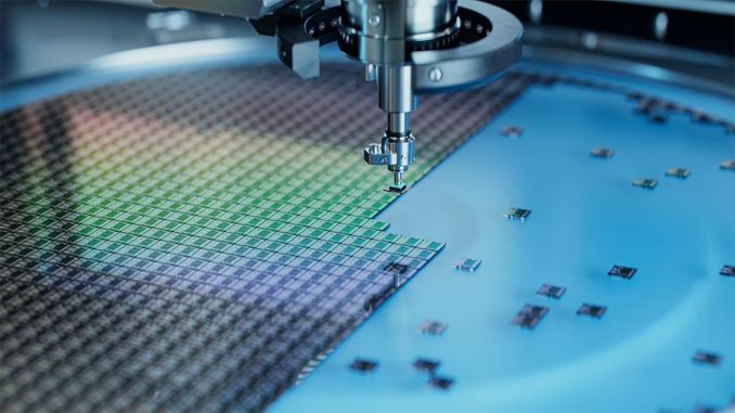
The network-attached storage (NAS) market had a break-out decade in the 2010s, with a large number of vendors trying to get a slice of the pie. Brands such as EMC / Lenovo and Thecus have fallen by the wayside, and even established storage vendors like Seagate decided to drop out of the market. QNAP and Synology have held firm in the commercial off-the-shelf (COTS) NAS market meant for home users, prosumers, SOHO, and SMB installations. ASUSTOR (backed by ASUS) has also been regularly releasing NAS units since their first product appeared in late 2012. TerraMaster released their first NAS around the same time, but opted to focus more on the direct-attached storage segment throughout the 2010s. The brand has shown renewed interest in the NAS market over the last few years. Despite the cut-throat competition in the COTS NAS market, some Asian vendors are attempting to get a toe-hold after establishing themselves in allied markets. UGREEN, a consumer electronics brand known for its power banks, chargers, USB adapters, and docks has also announced its entry into the NAS market, but we will cover that in a separate article.

Asustor, Buffalo, QNAP, Synology, TerraMaster, and Western Digital are currently the main options available for users looking to purchase a COTS NAS for SOHO / SMB use. Out of these, Buffalo and WD update their hardware options only once every 3 or 4 years. The others have a more regular cadence to their portfolio additions while continuing to maintain software support for the legacy units - sometimes even NAS units released as far as 10 years ago.

CES has usually been a good platform for NAS vendors, allowing them to show their latest and greatest in both hardware and software, and occasionally announce new models. However, the allure has been lost in recent years. It started with Synology and QNAP starting their own conference aimed towards partners / resellers and developers. Eventually, CES became relatively quiet for this market segment. Other business conferences focused on virtualization, security etc. are turning out to be better events for these NAS vendors. Overall, CES is no longer an important show for the NAS market. Having said that, the rest of this piece captures some of the announcements made in the NAS space around the 2024 CES time-frame.

At the 2024 CES, UGREEN made a big splash with the hardware options for their upcoming NASync series. Synology's booth rehashed units that have been around for a major part of 2023. A chuckle-worthy DS224+ (using an ancient Intel Celeron J4125) was also on display. ASUSTOR had a tiny presence in ASUS's suite, and the other NAS vendors gave the show a miss.

ASUSTOR Drivestor Lite and Drivestor 2/4 Pro Gen2 : Arm NAS with btrfs Support

ASUSTOR has updated their lineup of Arm-based NAS units for home / personal use, and the units are already available for purchase. The new Drivestor 2 Lite, 2 Pro Gen2, and 4 Pro Gen2 use a new Realtek processor - the RTD1619B. This is a quad-core Cortex-A55 SoC with the CPU running at 1.7 GHz. The Arm Mali-G51 MP3 in the SoC is clocked at 650 MHz. This lineup takes over the Drivestor 2, 4, 2 Pro, and 4 Pro units which had the Realtek RTD1296 (quad-core Cortex-A53 at 1.4 GHz). The increased processing power in the new processor, coupled with a new SDK from Realtek, has now allowed ASUSTOR to bring btrfs support in this lineup.

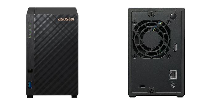
Despite using the same SoC, the Lite model differentiates itself from the Pro model by opting for half the RAM, and restricting itself to a 1 GbE LAN port (compared to the 2.5 GbE in the Pro ones). Two USB 3.2 Gen 1 Type-A ports in the Pro models are placed by a USB 2.0 port in the Lite model. There are two drive bays, but the drives themselves are not hot-swappable. ASUSTOR is promoting the transcoding performance of the new performance and portraying the Drivestor 2 Lite as a capable NAS for Plex and their own 'LooksGood' application.


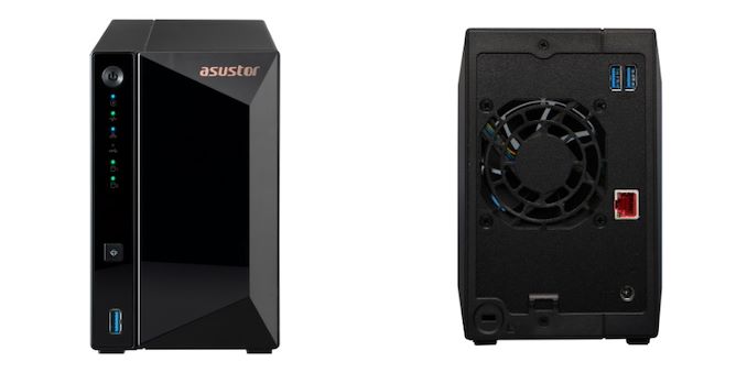
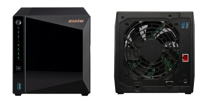
The Pro Gen2 models have hot-swappable bays. In addition to the hardware configuration updates, ASUSTOR is promoting a different set of applications such as Portainer (Docker) compared to the Lite model. The differences in the specifications are brought out in the table below.

ASUSTOR 2024 Drivestor Lineup
Model Drivestor 2 Lite Drivestor 2 Pro Gen2 Drivestor 4 Pro Gen2
ID AS1102TL AS3302T v2 AS3304T v2
SoC Platform Realtek RTD1619B
(4x Cortex-A55 @ 1.7 GHz / Arm Mali-G51 MP3)
RAM 1 GB DDR4 (Soldered) 2 GB DDR4 (Soldered)
OS Storage 8GB eMMC
Internal Storage / Bays 2x 3.5" SATA 4x 3.5" SATA
I/O Ports 1x USB 3.2 Gen 1
1x USB 2.0
3x USB 3.2 Gen 1
Network Ports 1x RJ-45 (1 GbE) 1x RJ-45 (2.5 GbE)
Power Adapter 65W (External) 90W (External)
Dimensions and Weight 165mm x 102mm x 218mm / 1.14 kg 170mm x 114mm x 230mm / 1.6 kg 170mm x 174mm x 230mm / 2.2 kg
Price $175 $269 $339

ASUSTOR has moved to the same platform adopted by Synology for the DS223 and other 23-series personal / home NAS models, keeping pace with the processing power offered by the competition. The introduction of btrfs support in this lineup now brings easy snapshots (and a bit of ransomware protection) to ASUSTOR's customers at an affordable price point.

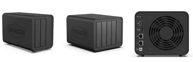
TerraMaster 424 and 424 Pro: High-Performance 2.5 GbE NAS Units with Alder Lake-N

TerraMaster recently updated their entry-level x86 NAS lineup for SOHO / SMB setups. This segment was served last year by the 423 series based on Jasper Lake (Celeron N5095). The 424 series utilizes Alder Lake-N. With Intel promoting an octa-core configuration as a Core i3 in this series, TerraMaster is also launching a 424 Pro utilizing the Core i3-N300.

The specifications of the three units are summarized in the table below.

TerraMaster 424 NAS Series (Alder Lake-N)
Model F2-424 F4-424 F4-424 Pro
SoC Platform Intel N95
(4x Gracemont @ up to 3.4 GHz / Intel UHD Graphics)
Intel Core i3-N300
(8x Gracemont @ up to 3.8 GHz / Intel UHD Graphics)
RAM 1x 8 GB DDR5-4800 SODIMM (Expandable to 1x 32 GB) 1x 32 GB DDR5-4800 SODIMM
Internal Storage / Bays 2x 3.5" SATA
2x M.2 2280 Gen3 x4 NVMe
4x 3.5" SATA
2x M.2 2280 Gen3 x4 NVMe
I/O Ports 1x USB 3.2 Gen 2 (Type-A)
1x USB 3.2 Gen 2 (Type-C)
Network Ports 2x RJ-45 (2x 2.5 GbE)
Power Adapter 40W (External) 90W (External)
Dimensions and Weight 222mm x 119mm x 154mm / 2.2 kg 222mm x 179mm x 154mm / 3.4 kg
Price $380 $500 $700

The TNAS operating system (TOS) is currently at 5.1, with the release of TOS 6.0 in the near future. Being a comparatively new entrant to the NAS world, the OS and mobile applications lack the polish of the offerings from established vendors, but the good news is that things can only improve from here. The hardware itself is quite capable, and the new 424 series is the first Alder Lake-N-based COTS NAS that we have seen for purchase. Terramaster had earlier experimented with a 10 GbE NAS using Apollo Lake, though it was unable to saturate that interface. The company seems to have opted for a more cost-effective platform with Alder Lake-N in the 424 series.

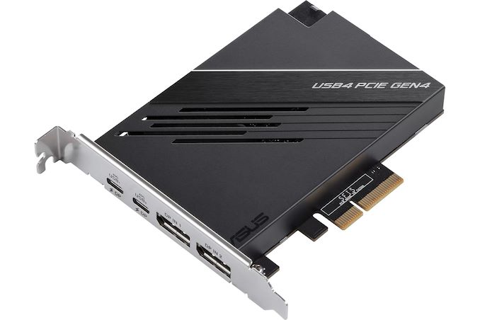
QNAP Ryzen 7000 Rackmounts, Wider TBS-h574TX NASBook Availability and Application Updates

QNAP remains busy throughout the year, regularly announcing hardware with the latest and greatest from Intel / AMD / ARM-based SoC vendors. The company also takes pride in updating different 'plugins' / first-party applications for their QTS / QuTS Here operating systems to increase their usefulness. Similar to Synology, the focus is slowly shifting more towards business users as a majority of their recent announcements have been related to their ZFS-enabled QuTS Hero-running NAS units.

At the 2023 CES, the company had teased their first consumer-focused hot-swappable all-flash NAS with M.2 / E1.S SSD support. The TBS-h574TX reached retail in late 2023, and QNAP uploaded a comprehensive video detailing the usage and features of the unit last month. After participating in the launch webinar prior to that, my expectations were tempered a bit. In the year since its teaser, the E1.S form-factor has not taken off as expected. Instead, we saw vendors like Solidigm and Micron focus on the traditional 2.5" form-factor with U.2 and U.3 SSDs. E1.L is making more sense for rackmount machines requiring very high storage density, but the general market trend seems to be more towards U.2 / U.3 for both consumer and SMB / SME on-premise usage. 2023 also saw the launch of 64TB-class U.2 / U.3 SSDs, and this form-factor seems widely available for purchase.

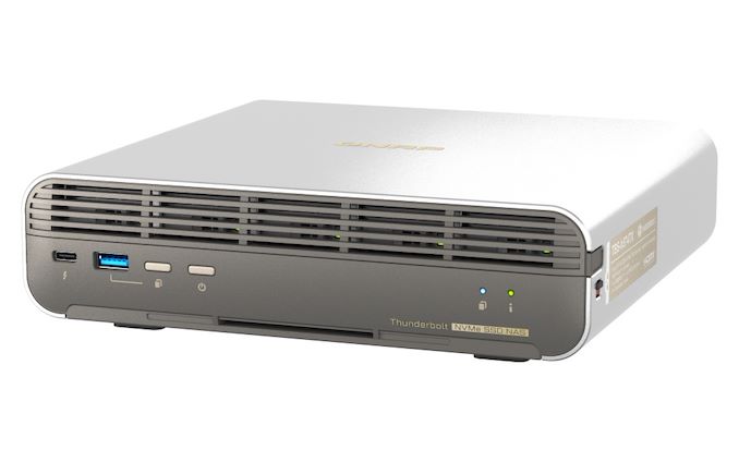
We believe that the M.2 form-factor in the NAS is better suited for caching and/or non-hot-swappable storage, while U.2 / U.3 makes more sense for hot-swappable units. QNAP pioneered the all-flash consumer NAS with the TBS-464 and ASUSTOR's Flashstor series made additional options available. The TBS-h574TX brings hot-swap into the picture, but some of the drawbacks of the designs still remain. For example, none of the SSD slots get the full four-lane capability, even though they physically accept x4 SSDs. QNAP contends that this is enough to saturate the 10GbE link, but that seems like a trade-off best avoided when it is possible to use the network port along with Thunderbolt (acting in IP mode with only 10 Gb capability per port) to have a 30 GbE up / 30 GbE down configuration. Single-slot occupancy can't deliver full performance in that configuration. In any case, QNAP believes their video production house customers will still find this unit delivering better performance than other options currently available in this form-factor, and they may be right on the practical front.

At $1200, this Raptor Lake-based system is not particularly cheap. Despite using an embedded part (Core i3-1340PE) which comes with in-band ECC support from Intel, QNAP doesn't have that enabled in the system (hopefully it is something that can be addressed in a future update). Overall, this product seems like a missed opportunity for QNAP in the all-flash consumer NAS market.

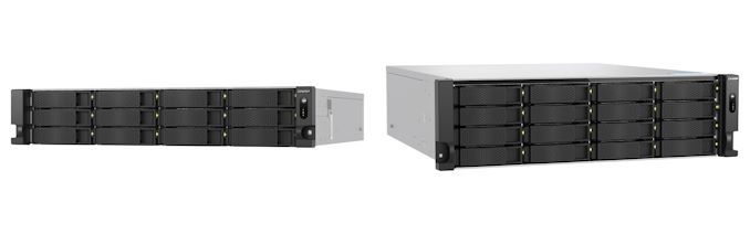
Moving on to the latest hardware introductions, QNAP is focusing more on ZFS-enabled NAS units now. The company recently introduced two rackmount units based on the Ryzen 7000 series, and their specifications are summarized in the table below.

QNAP TS-h77AXU-RP Series (Ryzen 7000 Series)
Model TS-h1277AXU-RP-R5-16G TS-h1277AXU-RP-R7-32G TS-h1677AXU-RP-R7-32G
Platform AMD Ryzen 5 7600
(6C/12T Zen 4 @ up to 5.1 GHz / AMD Radeon Graphics)
AMD Ryzen 7 7700
(8C/16T Zen 4 @ up to 5.3 GHz / AMD Radeon Graphics)
RAM (ECC UDIMMs Supported) 1x 16 GB DDR5-5200 UDIMM (Expandable to 4x 32 GB) 1x 32 GB DDR5-5200 UDIMM (Expandable to 4x 32 GB)
Internal Storage / Bays 12x 3.5" SATA
2x M.2 2280 Gen5 x2 NVMe
16x 3.5" SATA
2x M.2 2280 Gen5 x2 NVMe
I/O Ports 2x USB 3.2 Gen 2 (Type-A)
Network Ports 4x RJ-45 ([2x 2.5 GbE] + [2x 10GBASE-T])
PCIe Expansion Slots (Slot 1 + Slot 2): (Gen4 x4 + Gen4 x4) or (N/A + Gen4 x8)
Slot 3: Gen4 x4
Power Supply 550W x2
Dimensions and Weight (2U) 88.65mm x 432.05mm x 511.3mm / 13 kg (3U) 131.32mm x 482.09mm x 550.93mm / 15.64 kg
Price $3299 $3999 $4699

All models utilize 5GB of flash storage with dual-boot OS protection. ZFS support brings in deduplication and other features important for enterprise deployments. These are some of the first NAS units to support Gen5 M.2 SSDs (albeit, with x2 links), and QNAP advises use of their own heat-sink on them for use in these rackmounts. The redundant power supply configuration is also important in the use-case scenarios for these units, and the available expansion slots allows end users / IT administrators to add 25GbE network cards or SAS / SATA storage expansion cards as required. GPU pass-through is also supported, which can help specific virtualization setups where the VM and associated storage setup run on the same server block.

In software news from QNAP, the company is also promoting its machine-learning based drive failure prediction tool that uses a cloud-based engine beyond the traditional SMART readouts. It uses a third-party engine and requires a license purchase for use on more than one disk per NAS. QNAP is also touting its SSD anti-wear leveling features (QSAL) as a differentiating aspect of its QuTS ZFS operating system. These types of value-additions may help QuTS go head-to-head against options like TrueNAS.


from AnandTech https://ift.tt/H6597Ct
via IFTTT