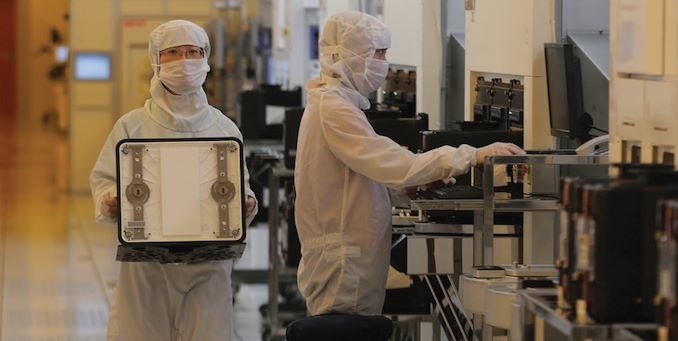
Samsung Foundry on Wednesday said that it had started production of chips using its 7LPP manufacturing technology that uses extreme ultraviolet lithography (EUVL) for select layers. The new fabrication process will enable Samsung to significantly increase transistor density of chips while optimizing their power consumption. Furthermore, usage of EUVL allows Samsung to reduce the number of masks it requires for each chip and shrink its production cycle.
The maker of semiconductors says that the 7LPP fabrication technology enables a 40% area reduction (at the same complexity) along with a 50% lower power consumption (at the same frequency and complexity) or a 20% higher performance (at the same power and complexity). As it appears, usage of extreme ultraviolet lithography enables Samsung Foundry to place 40% more transistors inside its next-gen SoCs and reduce their power consumption, a very compelling proposition for mobile SoCs that will be used by the parent company inside its future flagship smartphones.
| Advertised PPA Improvements of New Process Technologies Data announced by companies during conference calls, press briefings and in press releases |
||||||||
| 14LPP vs 28LPP |
10LPE vs 14LPE |
10LPE vs 14LPP |
10LPP vs 10LPE |
10LPU vs 10LPE |
7LPP vs 10LPP |
|||
| Power | 60% | 40% | 30% | ~15% | ? | 50% | ||
| Performance | 40% | 27% | >10% | ~10% | ? | 20% | ||
| Area Reduction | 50% | 30% | 30% | none | ? | 40% | ||
Samsung produces its 7LPP EUV chips at its Fab S3 in Hwaseong, South Korea. The company can process 1500 wafers a day on each of its ASML Twinscan NXE:3400B EUVL step and scan systems with a 280 W light source. The company does not say whether it uses pellicles that protect photomasks from degradation, but only indicates that usage of EUV enables it to cut the number of masks it requires for a chip by 20%.
This is a breaking news. We are adding details.
Related Reading:
- Samsung Foundry Updates: 8LPU Added, EUVL on Track for HVM in 2019
- Arm and Samsung Extend Artisan POP IP Collaboration to 7LPP and 5LPE Nodes
- Samsung Foundry Updates: 8LPU Added, EUVL on Track for HVM in 2019
- Samsung Foundry Roadmap: EUV-Based 7LPP for 2018, 3 nm Incoming
- Arm and Samsung Extend Artisan POP IP Collaboration to 7LPP and 5LPE Nodes
- Samsung’s 8LPP Process Technology Qualified, Ready for Production
- Samsung and TSMC Roadmaps: 8 and 6 nm Added, Looking at 22ULP and 12FFC
- TSMC Details 5 nm Process Tech: Aggressive Scaling, But Thin Power and Performance Gains
- TSMC Kicks Off Volume Production of 7nm Chips
from AnandTech https://ift.tt/2CQxXyO
via IFTTT